
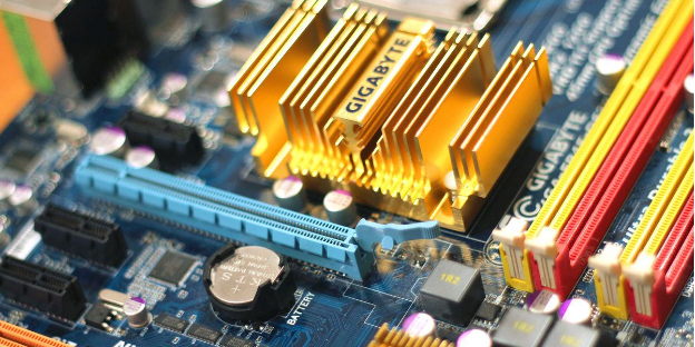
Every PCB assembly defect tells a story about a process that broke down somewhere, such as a stencil that wasn’t optimized, a reflow profile that wasn’t dialed in, or a component that wasn’t placed correctly. Knowing what common PCB assembly defects look like, why they happen, and how a good manufacturer prevents them is more than technical background. If you’re choosing an EMS partner, it can help you understand how carefully they work, how strong their quality process is, and how likely they are to catch problems before they affect your product.
Here are the defects that matter most in PCB assembly, and what actually prevents them.
Solder Bridges
A solder bridge is exactly what it sounds like: solder has connected two points on the board that were never supposed to touch. On a crowded PCB with fine-pitch components, that bridge can be extremely small and difficult to see, but the impact can be serious. It can create a short circuit, cause the board to fail, or lead to intermittent issues that are much harder to track down later.
Solder bridges often start early in the assembly process, especially during solder paste printing. Too much paste, a stencil that’s not properly aligned, or reflow settings that are not dialed in correctly can all create conditions where solder ends up where it shouldn’t be. That’s why prevention has to start before the board reaches final inspection. Stencil design, aperture sizing, solder paste inspection, and real-time process monitoring all help catch problems while they are still easy to correct. Once a bridge makes it through placement and reflow, fixing it becomes more time-consuming and more expensive.
At Sonic, we treat the solder paste printing stage as one of the most important points of quality control. Through stencil design review, automated solder paste inspection, and close process monitoring, our team works to prevent bridging before it has a chance to affect the finished assembly.
Tombstoning
Tombstoning is one of the easier PCB assembly defects to recognize. It happens when a small chip component, such as a resistor or capacitor, lifts up on one end during reflow. Instead of sitting flat on both pads, one side stands up like a tiny tombstone, leaving the lifted end without a proper electrical connection.
This usually comes down to uneven heating during the reflow process. If the solder paste on one side of the component melts before the other side, the surface tension from the melted solder can pull the component upright before the second side has a chance to connect properly.
Preventing tombstoning requires control over several details at once. The reflow profile needs to be carefully developed so components heat evenly. The preheat and soak zones also need to support a balanced temperature rise across the board. Pad design matters too, because uneven pad sizes can create uneven solder volumes and increase the risk of one side pulling harder than the other.
At Sonic, we look at tombstoning prevention through both process control and design review. Thermal profiling, accurate thermocouple placement, reflow profile adjustments, and DFM review all help reduce the risk before the board reaches production. The goal is simple: keep components flat, properly connected, and reliable in the finished assembly.
Cold Solder Joints
A cold joint happens when solder does not heat properly or does not have enough time to fully bond with the component terminal and the board pad. At first glance, the joint may look connected, but the connection can be weak. That creates risk for poor mechanical strength, higher electrical resistance, intermittent failures, and field issues that are difficult to trace later.
Preventing cold joints comes down to careful reflow profile control. The board needs to reach the right peak temperature and stay there long enough for proper solder wetting across the full assembly. That can be more complicated than it sounds, especially when a board includes components of different sizes, densities, and thermal mass.
At Sonic, reflow profiling is treated as an engineering process, not a generic setting pulled from a data sheet. By accounting for the full assembly and how heat moves across the board, our team helps prevent weak solder joints before they become reliability problems in the field.
Component Misalignment and Polarity Reversal
Placement accuracy says a lot about the quality of an SMT assembly process. When a component is placed even slightly off-center, the impact can vary. In some cases, the issue may be minor and cosmetic. In others, it can affect solder joints, electrical performance, or the long-term reliability of the board.
Polarity reversal is a separate issue, but it’s just as important to catch. This happens when a polarized component, such as a diode, electrolytic capacitor, or IC, is placed in the wrong orientation. Unlike minor misalignment, polarity reversal is always a functional problem. The board may not work at all, and in some cases, applying power can damage the component or surrounding circuitry.
Preventing placement and orientation defects requires control at several points in the assembly process:
- Accurate pick-and-place programming to ensure each component is placed in the correct position and orientation.
- Regular equipment calibration so placement machines continue operating within tight tolerances.
- Clear component markings and verified data to reduce the risk of orientation errors before production begins.
- Automated Optical Inspection after placement to catch misaligned parts before they move farther down the line.
- Automated Optical Inspection after reflow because some defects become easier to see only after soldering is complete.
- Inspection standards based on IPC-A-610 to evaluate alignment, pad coverage, orientation, and overall assembly acceptability.
At Sonic, placement accuracy is treated as a process control issue, not just an inspection checkpoint. The goal is to prevent alignment and orientation problems early, catch anything that does slip through, and protect board reliability before the assembly reaches the customer.
Solder Voids
Solder voids are small pockets of trapped gas inside a solder joint. The challenge is that they are not visible from the surface. In many cases, they can only be found through X-ray inspection, especially when the solder joint sits underneath the component.
Some minor voiding may be acceptable in standard assemblies if it falls within industry limits. But in high-reliability products, voiding can become a much bigger concern. Too many voids can weaken the solder joint and reduce thermal performance, which matters when the product needs to hold up in demanding conditions.
At Sonic, inspection is matched to the requirements of the product and the market it serves. AOI, X-ray inspection, and in-circuit testing are used based on customer quality standards, product risk, and end-use requirements. The goal is not to apply the same minimum inspection process to every board. It’s to use the right level of inspection to protect reliability where it matters most.
The Role of IPC Standards
PCB assembly defects are not judged in isolation. They are evaluated against accepted industry standards, and IPC-A-610 is the most widely used standard for determining whether an electronic assembly meets the required level of quality.
IPC-A-610 matters because not every product has the same performance expectations. A simple consumer device does not carry the same risk profile as a medical device, military assembly, or aerospace system. That’s why IPC-A-610 organizes assemblies into different classes based on how the product will be used.
The three IPC-A-610 classes include:
- Class 1: General electronic products where basic functionality is the main requirement and long-term reliability is less critical.
- Class 2: Dedicated service electronic products where continued performance and longer life are expected, but failure is not typically life-critical.
- Class 3: High-reliability electronic products where continuous performance is essential and failure could create serious consequences. This class is often used for medical, military, aerospace, and other mission-critical assemblies.
Knowing which class applies to your product should be one of the first conversations you have with your EMS partner. Inspection criteria, rejection thresholds, documentation requirements, and quality expectations all change depending on the class. The right EMS partner should be building to the requirements of your application, not applying the same baseline process to every board.
The Standard Your Product Deserves
The defects covered here represent the most common failure points in PCB assembly, and every one of them is preventable with the right process controls, inspection strategy, and EMS partner. The difference between a manufacturer who checks boxes and one who engineers quality into every stage of the build shows up in first-pass yield, in field return rates, and in the audit results that matter to your customers.
At Sonic Manufacturing Technologies, we build to the standard your application demands, whether that’s a Class 2 commercial assembly or a Class 3 high-reliability product destined for a medical device or defense system. Our process controls, inspection capabilities, and IPC-trained team are here to make sure what leaves our floor performs the way it should in the field.
If you’re evaluating EMS partners or have questions about how your specific assembly should be approached, contact Sonic Manufacturing Technologies at 510-826-5406. Let’s discuss what quality looks like for your product.