
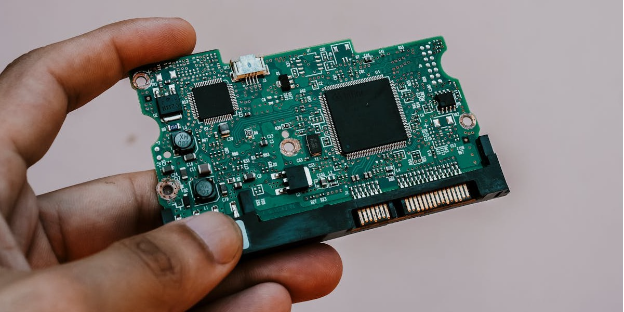
The promise of IoT devices is simple: connected devices should work reliably across many different environments with minimal human intervention. Sensors, controllers, and smart devices all need to collect data, communicate, and keep operating in the field.
But real-world conditions are often much less forgiving than a lab bench. Temperature changes, moisture, vibration, power fluctuations, and signal interference can all expose weaknesses in the hardware. When IoT devices fail in the field, the problem often traces back to the printed circuit board more often than product teams expect.
Understanding why IoT devices fail and how the decisions made during PCB design either create or prevent those failures is essential knowledge for anyone bringing a connected device to market.
The Unique Demands IoT Places on Hardware
IoT devices operate in environments that stress electronics in ways consumer products rarely face. Industrial sensors endure wide temperature swings, vibration, and humidity. Agricultural monitors sit outdoors through seasons of rain, heat, and cold. Wearables flex and compress thousands of times a day against the human body. Smart building devices run continuously for years without service.
At the same time, IoT products are often cost-sensitive, space-constrained, and expected to operate on minimal power for extended periods. That combination creates a set of engineering challenges that a well-designed PCB in IoT devices must anticipate and solve from the very beginning.
The Most Common Reasons IoT Devices Fail
Thermal Management Failures
Heat is the enemy of electronic longevity, and IoT devices that run continuously are especially vulnerable. When heat dissipation isn’t adequately planned during PCB design through proper component placement, thermal vias, and copper pours, components run hotter than they were rated for and their service life shortens accordingly. What looks like a random field failure in the field is often a thermal management problem that was baked into the design from the start.
Signal Integrity Problems
As IoT devices become more capable, they increasingly rely on high-speed digital communication between components. Poor PCB layout decisions can corrupt data, cause intermittent communication failures, and produce behavior that is nearly impossible to diagnose remotely. Signal integrity is not an afterthought. It’s a design discipline that must be applied from the first layout pass.
Power Supply and Regulation Issues
IoT devices frequently operate on battery power or harvest energy from the environment, making efficient and stable power delivery critical. A PCB layout that introduces noise into the power supply, places decoupling capacitors too far from the components they serve, or fails to adequately separate analog and digital power domains will produce erratic behavior. These failures are often intermittent and difficult to reproduce, which makes them among the most costly to diagnose and correct.
Mechanical and Environmental Stress Failures
Solder joint failures are a common reason IoT devices stop working in demanding environments. These failures can happen when a device is exposed to repeated temperature changes, vibration, or mechanical stress. Larger components may expand and contract at different rates as temperatures change. If the PCB design does not account for this, stress can build around the solder joints and eventually cause cracking. Placement also matters. Heavy components placed too close to the edge of the board are more likely to experience stress over time.
Inadequate EMI and ESD Protection
IoT devices transmit and receive wireless signals, which makes electromagnetic interference both a vulnerability and a compliance consideration. Boards that lack proper EMI shielding, inadequate grounding, or insufficient ESD protection on external-facing interfaces are susceptible to interference-induced failures and may fail regulatory certification. This is another costly problem to discover late in the development cycle.
Getting It Right Before It Goes Wrong
The failures described above share a defining characteristic: they are almost always preventable when the right expertise is applied early in the design process. Design for manufacturability reviews, thermal simulation, signal integrity analysis, and close collaboration between the design team and the contract manufacturer before a single board is fabricated can surface and resolve the issues that cause field failures.
At Sonic Manufacturing, we work with IoT product teams across the full development lifecycle — from DFM review and prototyping through scaled production — to build the kind of hardware reliability that connected devices demand. The environments IoT devices operate in are unforgiving. The PCB designs that go into them shouldn’t leave anything to chance.
If your team is developing an IoT product and looking for a manufacturing partner with the expertise to get it right the first time, we’d welcome the conversation. Reach out to our team today at 510-826-5406 to request a free quote.