
When you work with a printed circuit board (PCB) manufacturer like Sonic, it’s helpful to understand some of the lingo so that you can form an effective partnership. Even though your PCB manufacturer will be handling many aspects of the project, communication is important for both parties. For instance, you’ll want to discuss your needs and timeline with your manufacturer so that they know what you expect and when. Regular communication also ensures the manufacturer is on track to meet your goals.
Since there is a lot of lingo in the PCB world, we thought it would be helpful to share some of the key PCB terms to know. By understanding these terms, you’ll have the confidence you need to discuss your next project. Let’s dig in!
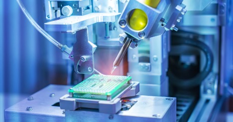
Key PCB Terms to Know
Components
Components are the functional parts attached to the PCB. These include resistors, capacitors, transistors, and integrated circuits, each playing a specific role in the board’s operation.
Conductors and Traces
Conductors are fine copper lines that connect different components, allowing electrical signals to travel where they’re needed. Think of them as the electrical pathways on a PCB.
Copper Pour
Copper pour refers to larger areas of copper on the board, usually used for grounding or to connect multiple components efficiently. It helps with electrical performance and heat management.
Gerber Files
Gerber files are the detailed digital maps manufacturers use to create a PCB. They specify everything from copper layers to drill holes to silkscreen markings.
Printed Circuit Board (PCB)
A PCB is a sturdy, flat board made from a non-conductive material, usually fiberglass-reinforced epoxy. It supports and connects all the electronic components in a system.
Silkscreen
The silkscreen is the printed layer on the PCB that shows component labels, logos, and other important information, helping guide the assembly and maintenance process.
Soldering
Soldering joins components to the PCB using a heated metal alloy. A good solder connection ensures electrical continuity and mechanical strength.
Surface Mount Technology (SMT)
Surface mount technology involves mounting components directly onto the surface of the PCB. This method allows for more compact and efficient board designs.
Through-Hole Technology (THT)
An alternative to SMT, through-hole components have leads that are inserted into drilled holes and soldered to the board. This method offers greater durability, especially for larger or high-stress components.
Via
A via is a tiny hole that allows electrical signals to pass between different layers of a PCB. It’s essential for connecting circuits on multi-layer boards.
Additional PCB Terms to Strengthen Your Knowledge
Are you with us so far? If you’ve brushed up on the terms above, here are some more helpful ones to know when discussing your upcoming PCB project.
Bill of Materials (BOM)
The BOM lists every component needed for a PCB project, including quantities and specifications. It’s the essential checklist for manufacturing.
Circuit Layer
Each circuit layer contains a set of traces and connections. Multi-layer PCBs stack several circuit layers to handle more complex designs.
Copper Weight
Copper weight measures the thickness of copper on the PCB, typically in ounces per square foot. Thicker copper can carry more current and provide better heat dissipation, making it ideal for certain PCB projects.
Design Rule Check (DRC)
A DRC is an automated review process that ensures a PCB design complies with manufacturing standards and avoids costly errors.
Footprint
A footprint defines the space a component occupies on the PCB, including the placement of solder pads and holes. Accurate footprints are critical for proper assembly.
Ground Plane
The ground plane is a large area of copper connected to the circuit’s ground. It stabilizes voltage levels and reduces electromagnetic interference.
Power Plane
Similar to a ground plane, the power plane distributes voltage across the PCB, supplying energy efficiently to various components.
Schematic
A schematic is the visual diagram of a PCB’s electrical connections. It’s the blueprint used during both design and troubleshooting.
Solder Mask
The solder mask is a protective coating that covers the PCB’s surface, except where soldering is needed. It prevents accidental shorts and protects against environmental damage.
Trace Width and Spacing
Trace width and spacing determine how much current a PCB trace can handle and how closely traces can be placed without causing electrical interference.
Building Your PCB Confidence
Understanding these key concepts will make it easier for you to collaborate with your PCB manufacturer, ask informed questions, and ensure the final product meets your expectations.
But remember, you don’t need to be a PCB expert to bring your project to life.
Our team at Sonic is here to guide you every step of the way. Whether you need custom design support, prototyping, or full-scale production, we’re ready to help. Contact us today at 510-826-5406 to discuss your project needs.