
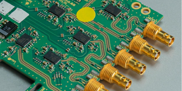
The most problematic failures in electronics manufacturing are the ones that don’t show up during production. Even boards that pass visual inspection, automated optical inspection, and functional testing can still carry defects that cause the product to fail months after it reaches the consumer. Fortunately, burn-in testing helps find these failures before they leave the facility.
For manufacturers in high-stakes industries like aerospace, medical devices, IoT infrastructure, and wearables, understanding burn-in testing is important. Let’s learn more about what burn-in testing is, the issues it catches, and when it’s non-negotiable.
What Burn-In Testing Actually Does
Burn-in testing is a reliability screening process that operates electronic components under elevated stress conditions, typically increased temperature, voltage, or both. The goal is to accelerate early-life aging and force hidden defects to show themselves in a controlled environment before the product reaches the customer.
This process is grounded in what reliability engineers call the bathtub curve. This is the well-established pattern in which electronic components often experience a higher failure rate early in their life, followed by a long period of stable operation, and then another increase in failures near the end of their useful life.
Burn-in testing targets that early failure window, often referred to as infant mortality. By moving devices through this higher-risk stage before shipment, manufacturers can identify components that are likely to fail prematurely.
A device that survives a properly designed burn-in protocol has demonstrated that it can withstand expected stress conditions and move beyond its most vulnerable early-life period. The result is a more reliable product, stronger quality control, and greater confidence that what ships has already been tested under demanding conditions.
The Issues That Burn-In Testing Catches
The defects burn-in testing catches are not always obvious. They are often the hidden failures that standard inspections and functional testing may miss because they only appear after a device has been exposed to sustained operating stress. In other words, the component may work during a basic test but fail once heat, voltage, time, or continuous operation begin to reveal underlying weaknesses.
Burn-in testing is designed to uncover issues such as:
Marginal or Defective Components
A capacitor, resistor, or semiconductor that is technically within spec but at the edge of its acceptable range will often reveal itself under thermal or electrical stress. These are components that would pass incoming inspection but fail prematurely in the field.
Latent Solder Joint Defects
Cold solder joints, insufficient wetting, and micro-voids that aren’t visible during inspection can become permanent failures when subjected to thermal cycling. Burn-in puts those joints through stress that reveals their weakness before the product is deployed.
Thermal Design Issues
Running a device at elevated temperature under load can expose inadequate heat dissipation, hot spots on the board, or component interactions that weren’t apparent during design validation. For densely populated boards or devices that will operate in warm environments, this is especially valuable.
Intermittent Failures
Some of the most difficult defects to diagnose are the ones that only appear occasionally. Extended burn-in operation increases the probability that an intermittent failure will manifest during testing, where it can be identified and addressed, rather than in the field, where it creates a warranty claim and an unhappy customer.
When Burn-In Testing Is Warranted
Burn-in testing adds time and cost to the manufacturing process, so the decision to include it should be based on a clear understanding of the application and its risk profile. It’s most clearly warranted in several scenarios.
- For medical devices and aerospace applications, where a field failure can have direct consequences for patient safety or mission success, burn-in is often a regulatory or contractual requirement.
- For IoT devices deployed in large volumes across distributed locations, the cost of field failures frequently exceeds the cost of burn-in by a significant margin.
- For wearables and consumer electronics that are difficult to service after deployment, catching infant mortality failures in the factory is far more cost-effective than managing returns and replacements at scale.
The calculus is simpler than it might appear: if the cost of a field failure in warranty claims, recalls, liability, or brand damage exceeds the cost of burn-in testing, burn-in testing is the right investment.
Building Quality In, Not Testing It In
At Sonic Manufacturing, burn-in testing is one component of a broader approach to electronics manufacturing quality that begins at design for manufacturability and runs through every stage of production. Our team works with clients across aerospace, medical, IoT, wearables, and industrial markets to develop testing strategies that match the risk profile of their specific application.
If you’re evaluating your current testing strategy or looking for a contract manufacturing partner who treats quality as a core competency, we’d welcome the conversation. Contact us today 510-826-5406 for a free quote.