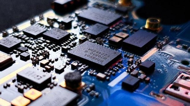
Advanced thought is required to build high-speed circuitry. Without a proactive approach, it will be extremely difficult to get the speeds you’re looking for. High-speed PCB design focuses on creating circuit boards that are less vulnerable to signal integrity, power integrity, and EMI/EMC problems.
While no design is ever completely free of these issues, there are things PCB designers do to reduce them to an unnoticeable degree. This way, they won’t cause problems in the final product. Below are some key PCB design considerations for high-speed digital circuits.
Stackup and Impedance
The PCB stackup will determine the impedance and ease of routing. All PCB stackups include a set of layers that are responsible for signal, power, and ground planes. When assigning the layers, it’s important to account for the board’s size, routing density, interfaces, power integrity, and low speed and RF signals.
Materials, Layer Count and Thickness
There are several ways to determine the layer count needed to accommodate all the digital signals in your design. They’re based on math and experience, which fortunately, is not a problem for Sonic’s PCB design experts!
As for materials, there are certain materials that work best for high-speed applications such as FR4-grade materials, PTFE-based laminates, and spread glass laminates. FR4-grade materials are ideal for when the routes between components are not too long. If they do become too long, you may need a more specialized material like PTFE-based laminates.
Routing and Signal Integrity
Signal integrity starts with designing to a specific impedance value and then maintaining this during layout and routing. Other strategies that can be used to ensure signal integrity include:
- Always aim for shorter routes between components
- Minimize routing through vias
- Eliminate stubs on ultra-high speed lines
- Prevent signal reflection with termination resistors
- Choose the proper materials and processes
Power Integrity
Ensuring stable power delivery to high-speed components is also critical, as power integrity issues can sometimes mimic signal integrity problems. When done right, power is delivered to fast components with low noise. The PCB stackup will help with this, as it allows the designer to determine the level of power integrity in the design. This ensures low emissions, low noise, and the elimination of signal integrity problems, which are all important PCB design considerations for high speed digital circuits.
Routing
Naturally, routing plays a crucial role in high-speed design, as it affects the spacing, impedance and length targets. While there are many guidelines to follow, one of the most important is to place ground planes near your traces. This maintains consistent impedance and ensures a clear return path is defined in the PCB layout.
High-Speed PCB Design
Sonic Manufacturing Technologies was established in 1996 and is the largest EMS in Silicon Valley. We have seasoned technical staff, fast turnaround times and a ‘can do’ attitude that sets us apart from others in the industry. To discuss your needs for a high-speed printed circuit board, contact our team of PCB experts today.

